
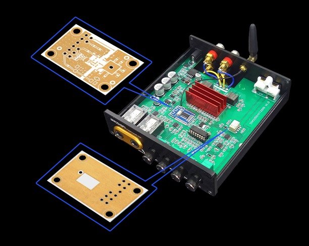

A bare ceramic board is only half the story. Assembly is the stage where it gets mounted with components and turns into a working device, which is why ceramic PCB assembly sits so close to the performance of the final product. The site describes assembly as mounting bare boards with electronic components to make semi-finished devices, covering both PCBA manufacturing and PCBA tests.
Where High-Performance Boards End Up
BSTCeramicPCB Co lists ceramic boards in high-power semiconductor modules, IGBT modules, 5G communication electronics, medical equipment, aerospace and national defense systems, among other fields. Products like these leave little room for a poorly built assembly, so the process behind it deserves a closer look.
Paste and Placement
The line starts with solder paste. A fully automatic stencil printer and squeegee spread it across the board, and the paste then connects surface components to the pads while providing electrical and thermal connections. It also removes the need for solder wire. A 3D SPI detector checks the paste before any component goes down, so insufficient or excessive solder is caught early. After that, SMT equipment places components in position according to the design drawings. The site is careful to point out that SMT is a process, while SMD only refers to the components themselves.
Reflow and Inspection
Reflow soldering then fixes the surface-mount components to the substrate. The site notes that solder particles can oxidize during air reflow, which can leave a cosmetic defect known as graping. Afterwards, AOI cameras scan the board for missing components and quality defects, and X-ray inspection is listed for mass production runs. After AOI, defective boards are repaired by hand in touch-up, for example for poor connections, and cleaning combines mechanical equipment with manual work. Manual soldering handles leaded components and is generally used for small production runs, lab assembly work, rework and repair, and adding extra components to a machine-soldered board.
Testing Around the Assembly Steps
Several checks sit around the assembly steps themselves:
- First piece testing: the first product of a run is examined against design specifications and engineering drawings
- IC programming: loads a program into the IC so the circuit can operate normally
- Functional testing: checks that each component meets the standard, including resistors, sensors, and capacitors
- Thermal aging testing: tests how well components withstand extreme temperatures for long periods, since differences in thermal expansion can eventually cause failure
The Bigger Quality Picture
The site says PCBA tests run through the whole process, and the assembly page ties these steps into the company’s wider quality system, pointing to raw materials guarantee, pre-production inspection, and rigors testing and inspection. It also lists ISO, IATF, REACH, RoHS, and UL compliance and mentions BOM check, first article inspection, and functional testing as part of the process. The page also links inspection data reports for stages including paste printing, SMT, nitrogen reflow soldering, AOI, manual soldering, X-ray, cleaning, and IC programming, so the process can be reviewed stage by stage.
Getting Started
Getting started is simple enough. Customers send a Gerber file and, when assembly is needed, a BOM. BSTCeramicPCB Co’s ceramic PCB assembly page describes a one-stop service run from its own PCBA factory, and the homepage says quick turn-out is available.
Worth Asking About
Ceramic PCB assembly is where design intent meets real components, so the checks before, during, and after placement matter as much as the board itself. Asking a supplier to walk through each stage is a sensible first step.